In the field of traditional semiconductors, the different conductivity types of materials usually come from different impurity doping, and it is impossible to achieve the conversion of conductivity behavior through electricity. In a bipolar two-dimensional semiconductor, electrons and holes can be transported in the channel at the same time, and their conduction behavior is not only regulated by the gate voltage, but also largely affected by the source and drain voltages. This effect is particularly obvious in devices with thin gate dielectric layers, which can provide a new way for the design of reconfigurable circuit chips in the future. Professor Jun He’s group has been engaged in the research of bipolar two-dimensional semiconductor devices for a long time, including the interface regulation of bipolar two-dimensional semiconductor conductivity (Adv. Mater. 2019, 31, 1901144; Adv. Mater. 2019, 31, 1805317 ) And dynamic regulation of the conduction behavior of bipolar two-dimensional semiconductor heterojunctions (Adv. Funct. Mater. 2019, 29, 1804897; Nat. Electron. 2018, 1, 356-361), etc. Recently, the international authoritative journal Advanced Materials ("Advanced Materials") published online the new progress made by Professor Jun He's group in the direction of bipolar two-dimensional semiconductor devices. The title of the paper is "Modulation of Negative Differential Resistance in Black Phosphorus Transistors" ("Negative Differential Resistance Modulation in Black Phosphorus Transistor"). The School of Physics and Technology of Wuhan University is the only communication unit for this research. Professor Jun He is the corresponding author, and Associate Researcher Cheng Ruiqing is the first author.
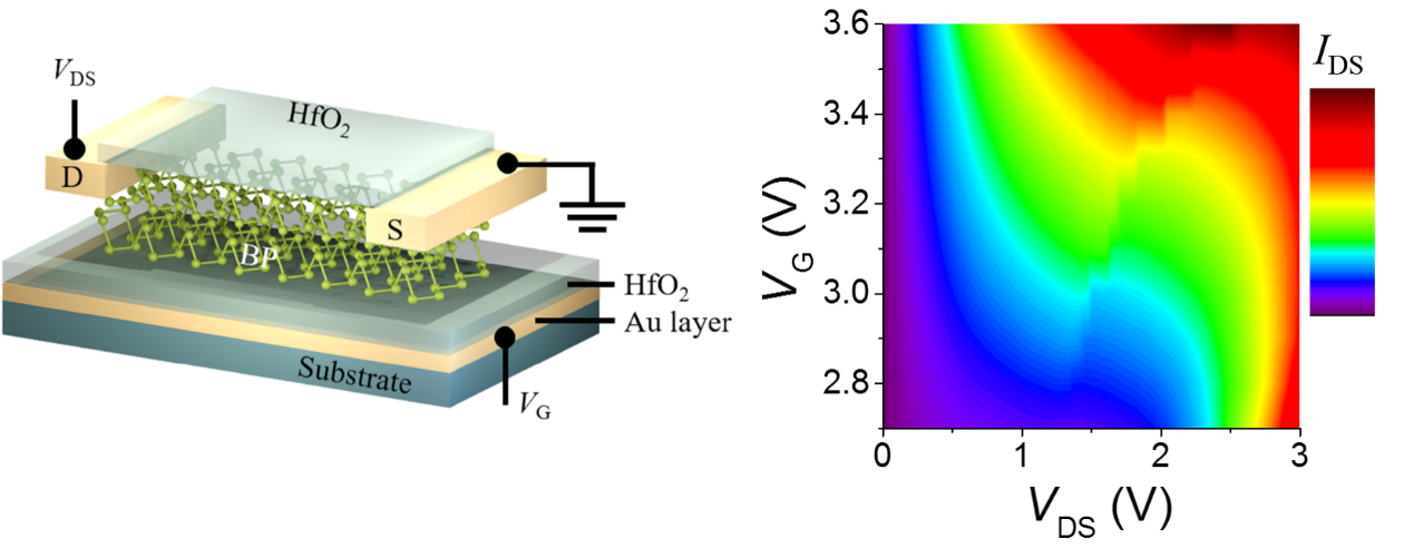
In this research work, He Jun’s research group used the specific electric field dependence of the lateral carrier distribution in the bipolar channel to achieve room temperature negative differential resistance (NDR) in a two-dimensional black phosphorus field effect transistor based on a thin gate dielectric layer. )characteristic. Different from traditional negative differential resistance devices based on quantum tunneling effect, the negative differential resistance phenomenon in black phosphorous transistors originates from the switching of carrier types in the bipolar conduction channel under specific electric field conditions. It is impossible to achieve in device configuration. The black phosphorus negative differential resistance device exhibits an ultra-high peak current density (~34 μA/μm) and excellent gate voltage regulation capability. Due to the different injection methods of the two types of carriers (electrons and holes), their NDR and Kink characteristics (that is, the phenomenon of abnormal current increase) show different temperature dependence from traditional negative differential resistance devices. In addition, the device also exhibits excellent optical tunability, not only can effectively regulate the peak current and peak voltage, but also can induce NDR characteristics through light when the dark state does not exhibit NDR characteristics. The above research results will help us understand the conduction behavior of bipolar two-dimensional semiconductors, and provide new ideas for related electronic applications such as radio frequency and logic.
The research work was supported by the National Key Basic Research and Development Program, the National Natural Science Foundation of China and other projects.

Schematic diagram of device structure and negative differential resistance characteristics
Original link:https://doi.org/10.1002/adma.202008329