The two-dimensional layered semiconductor layer is formed by strong covalent bonds or ionic bonds, and the layers are stacked by weak Van der Waals forces. There are no chemical dangling bonds on the surface, so that the carriers are free from the influence of the scattering mechanism caused by surface roughness and charge center, so as to obtain a higher carrier mobility. But its ultra-thin characteristics lead to a small absorption cross-section; weak electrostatic shielding effect leads to a large exciton binding energy in two-dimensional materials; and strong Coulomb interactions will also increase photo-generated electrons and holes in defects through the Auger process. The compound probability of the place. These shortcomings all limit the application of two-dimensional materials in photodetection.
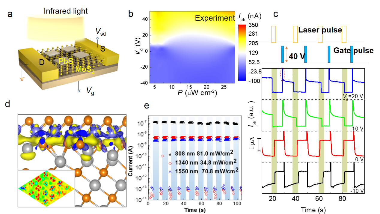
In order to overcome these shortcomings of two-dimensional layered materials, and use the high-efficiency light absorption properties of non-layered chalcogenide narrow band gap semiconductors. He Jun's research group realized an infrared non-volatile memory based on MoS2/PbS van der Waals heterojunction. The photo-generated electrons and holes are spatially separated, and the device effectively prevents the recombination of photo-generated electrons and holes, and greatly improves the photoconductor gain. The device exhibits extremely high infrared light detection performance: the light responsivity exceeds 107 amperes per watt, the optical gain exceeds 1011, the detection rate exceeds 1015 Jones, and it has extremely stable optical storage performance with a storage time of more than 104 seconds. In addition, the memory can be erased by pulsed grid voltage and remains stable after 2000 cycles. Combining theoretical models and experimental data, we found that the optical storage mechanism comes from the injection of photogenerated electrons in PbS into MoS2, and the interface barrier ФR prevents electrons in MoS2 from being injected back into PbS. The photo-generated holes are localized in the PbS to cause a grating effect, and the induced electron concentration is about 2.4×1024cm-3, and the phenomenon of optical storage appears. The electron concentration of MoS2 increases through the pulse gate voltage, and the electrons in MoS2 are injected into PbS through quantum tunneling to recombine with the local holes, and the optical storage is erased. This research result provides new ideas for optoelectronic storage and its logic circuits. The related research results are published in science advances (Sci. Adv. 2018; 4: eaap7916) under the title "Nonvolatile infrared memory in MoS2/PbS van der Waals heterostructures". superior.
On the basis of the research on the controllable preparation of van der Waals heterojunction and its electronic and optoelectronic properties, it is found that the vdW gap in the van der Waals heterojunction can induce strong orbital hybridization between the S dangling bonds on the surface of the narrow band gap semiconductor PbS and the artificially induced S vacancies in MoS2. Come to bridge. In the vdW heterostructure, the additional tunneling barrier introduced by the vdW gap greatly increases the injection barrier of photogenerated carriers. Through this seamless bridging strategy, the device exhibits extremely high detection performance in the near-infrared band. The gapless heterostructure constructed by He Jun's research group realizes fast optical switching without the use of pulsed gate voltage. The bridged MoS2/PbS heterostructure has an ultra-high light-triggered on/off ratio (over 106) and ultra-fast response. The speed is 47μs. Compared with similar vdW phototransistors, this gapless heterostructure phototransistor has significantly improved light trigger switching ratio and light response time (response speed increased by more than 5 orders of magnitude; response speed increased by more than 4 orders of magnitude) . Relevant research results have been published on ACS Nano (ACS Nano 2019, 13, 14519−14528) with the title "Gapless van der waals heterostructures for infrared optoelectronic devices".
Paper link:http://advances.sciencemag.org/content/4/4/eaap7916/tab-pdf
https://pubs.acs.org/doi/pdf/10.1021/acsnano.9b08375

MoS2/PbS structure diagram and infrared photoelectric transport