1. Van der Waals epitaxial growth of two-dimensional materials
In recent years, a new type of two-dimensional electronic material represented by graphene (G) and molybdenum disulfide (MoS2) has important characteristics such as ultra-thin thickness, smooth surface without dangling bonds, and can be stacked arbitrarily. On the premise of not increasing the area of the device, it overcomes the physical quantum effect and greatly improves the density and performance of the transistor. Therefore, two-dimensional materials have become important candidates for the next generation of high-density integrated circuits, and they are the core force for realizing the integration of multi-functional, high-performance devices with new principles. However, there is still an important problem that limits the large-scale application of two-dimensional materials is how to achieve mass controllable production of high-quality two-dimensional materials. The existing preparation methods, such as the samples obtained by the peeling method, have problems such as small domain size, uncontrollable thickness, and difficulty in obtaining a uniform large area. Therefore, if you want to realize the large-scale integrated application of heterogeneous devices based on two-dimensional materials, the epitaxial growth of high-quality large-area two-dimensional materials and the construction of heterostructures are the first problems to be solved.
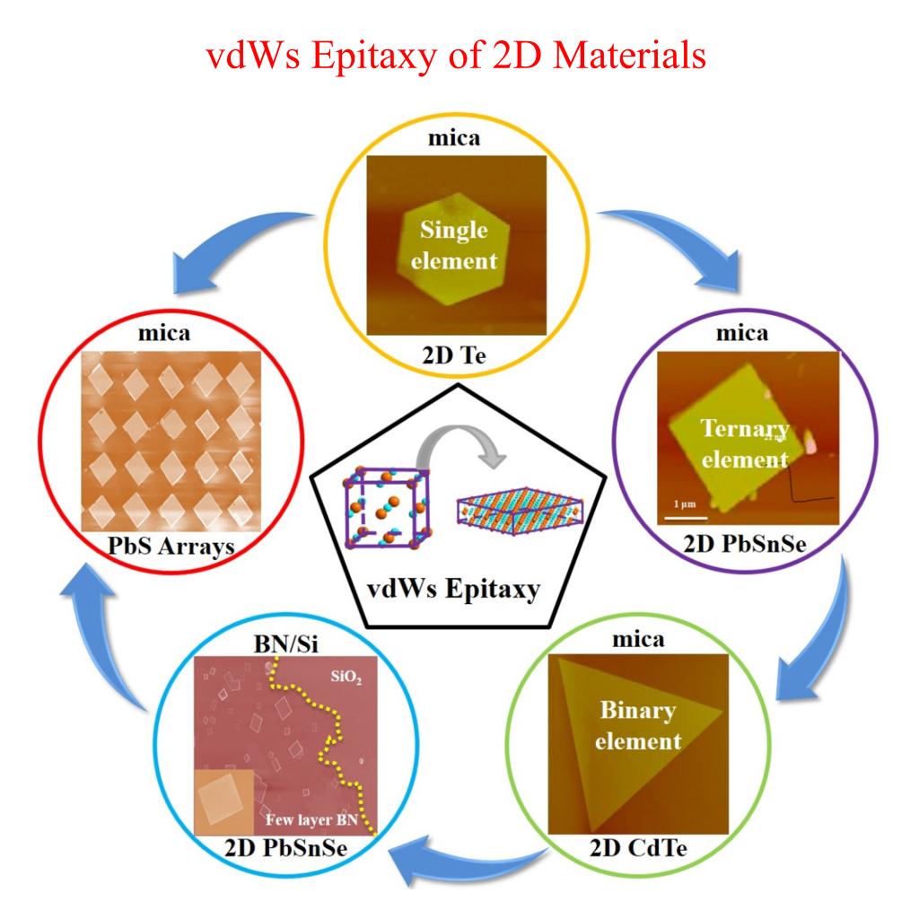
In recent years, our research group has applied van der Waals epitaxy to the two-dimensional growth of non-layered chalcogenide semiconductor materials, from hexagonal crystal to cubic crystal structure, from single component to complex three-component system, and realized CrSe and CdTe respectively. , Pb1-x SnxSe, PbS, NbS2, Bi2O2Se, Te, Cr2S3, α-MnS and other non-layered materials with different crystal structures two-dimensional and array structure. At present, a series of research progress has been valued by international colleagues, including 5 Advanced Materials (Adv. Mater. 2019, 31, 1900056; Adv. Mater. 2017, 29, 1703122; Adv. Mater. 2016, 28, 617; Adv. Mater. 2016, 28, 6497; Adv. Mater. 2016, 28, 8051-8057), 1 Nano Letters (Nano Lett. 2019, 19, 2154-2161); 2 ACS Nano (ACS Nano 2019, 13 , 1451914528; ACS Nano 2019, 13, 12662-12670).
The emergence of two-dimensional ferromagnetic materials provides an unprecedented opportunity for people to study the magnetic properties of materials with atomic layer thickness, and its emergence provides the possibility for the design of two-dimensional spintronic devices. However, a common problem existing in two-dimensional ferromagnetic materials is that the Curie temperature (Tc) of two-dimensional ferromagnetic materials is dominated by the magnetic coupling between layers. Tc decreases as the thickness decreases and is much lower than room temperature, which is obviously not conducive to It is used in actual spintronic devices. Recently, based on the research of the controllable preparation of van der Waals epitaxy method, our research group has successfully realized the large-area preparation of Cr2Te3 single crystal with 1 to 2 unit cell thickness. Through further research, we found that when the Tc of Cr2Te3 changes from 160 K in the bulk material to 5-6 unit cell thickness, its Tc will rise sharply to 280 K, magnetization and anomalous Hall effect (AHE) The measurement provides clear evidence for the existence of spontaneous magnetization at room temperature. The theoretical model indicates that the surface reconstruction of Cr2Te3 may be the origin of the abnormal thickness dependence of Tc. This size modulation method opens up a new way to manipulate ferromagnetism (Nano Lett. 2020, 20, 3130−3139).
2. Advanced multi-function devices based on two-dimensional
So far, two-dimensional materials have been proven to have broad application prospects in logic devices, memory devices, and optoelectronic devices. In addition, different two-dimensional materials can be stacked freely with the help of weak van der Waals force to form an artificial heterostructure with an atomic level flat interface. This heterostructure is usually called a van der Waals heterojunction. By choosing different two-dimensional materials and specific stacking methods, their unique properties can be organically combined. From this research perspective, van der Waals heterojunction provides a new platform to study the properties of new electronic and optoelectronic devices.
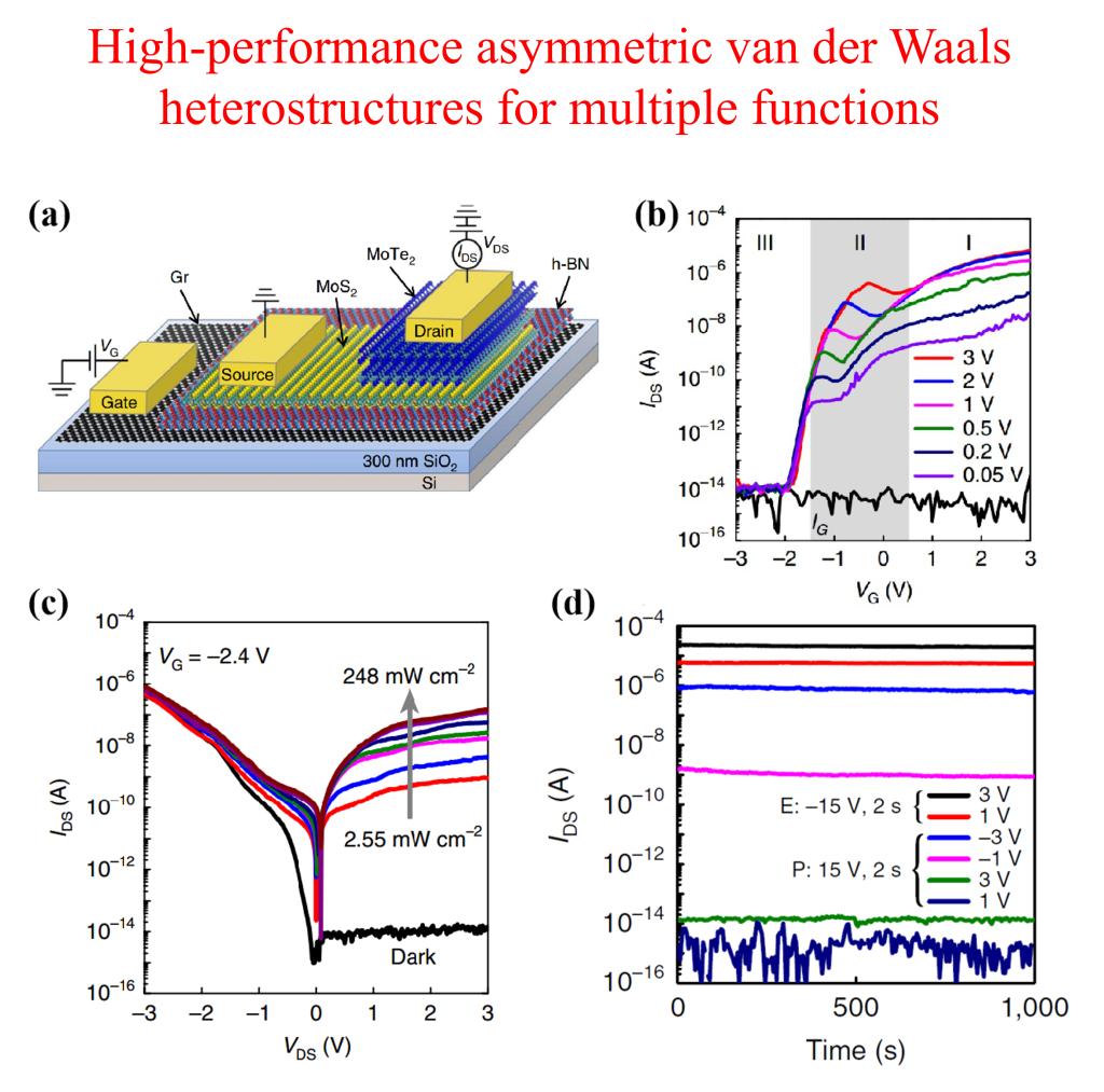
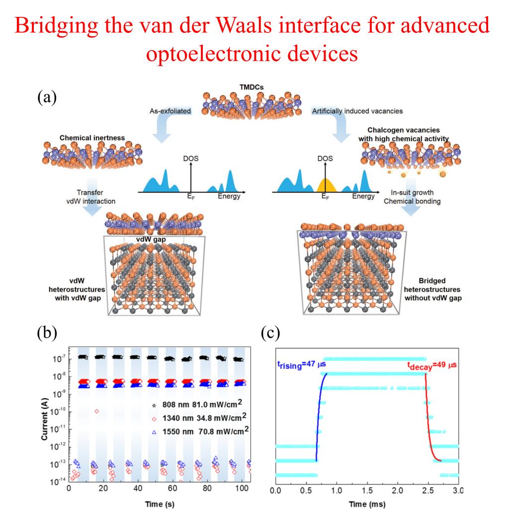
While studying the growth of two-dimensional materials, our research group is also committed to designing two-dimensional multifunctional electronic devices. At present, a series of research results have been achieved in this direction: (1) We have successfully built graphene, h-BN, The asymmetric van der Waals heterojunction device composed of MoS2 and MoTe2 realizes a high-performance multifunctional integrated optoelectronic device. Due to the asymmetric structure of the device, charge carrier injection can be switched between tunneling and thermal activation under positive and negative bias conditions, respectively. Therefore, the device not only has a high current switching ratio (6×10⁸) and a rectification ratio (~108), it can also be used as a programmable rectifier with stable maintenance and continuously adjustable storage state, which exhibits ultra-high reading and writing And erase current ratio (~109) and rectification ratio (~107). This research has achieved the organic unification of ultra-high device performance and multi-functional integration, and provided new ideas for exploring high-performance heterogeneous devices with new principles. The results have been published in Nat. Electron., 2018, 1, 356. (2) The logic function of a unipolar memristor made of HfSe2-xOx sheet was demonstrated for the first time, and memtransistors were built using MoS2/graphene/HfSe2−xOx van der Waals heterostructure. Double-ended memristive resistors have stable unipolar switching characteristics, high switching ratio (>106), high operating temperature (106°C), long-term durability (>104 s) and multi-bit data storage, and can be used as a storage lock Registers and logic gates. Thanks to these excellent memory characteristics, the three-terminal heterostructure memory transistor exhibits extensive tunability in electrical switching behavior, and can simultaneously realize logic operations and data storage. Finally, we discussed their application prospects in logic units with storage capabilities such as D-type flip-flops. These results show the potential of two-dimensional materials in resistive switch applications and open a way for future memory calculations (Nano Lett. 2020, 20, 4144−4152). (3) Using MoS2, h-BN, and CuInP2S6 (CIPS), a two-dimensional double-gated ferroelectric van der Waals heterojunction is constructed, which can be used as a high-performance non-volatile memory and a programmable rectifier. Due to the insertion of h-BN and the dual-gate coupling configuration, the ferroelectricity of CIPS can be effectively regulated and stored stably. Through this design, the device has shown record high performance as a non-volatile memory. It has a large memory window, a large switching ratio (107), ultra-low programming current (10−13 A), and long-term durability. Performance (104 s); As a programmable rectifier, we have observed a wide range of gate adjustable rectification behavior, and the device has a large and stable rectification ratio (3×10⁵) in the programmed state. This study shows the potential of ferroelectric van der Waals heterojunctions in new multifunctional ferroelectric devices (Adv. Mater. 2020, 32, 1908040). (4) On the basis of the research on the controllable preparation of van der Waals heterojunction and its electronic and optoelectronic properties, it is found that the vdW gap in the van der Waals heterojunction can pass through the narrow band gap semiconductor PbS surface S dangling bond and the artificially induced S vacancy in MoS2. The tracks are hybridized to bridge. In the vdW heterostructure, the additional tunneling barrier introduced by the vdW gap greatly increases the injection barrier of photogenerated carriers. Through this seamless bridging strategy, the device exhibits extremely high detection performance in the near-infrared band. The gapless heterostructure constructed by He Jun's research group realizes fast optical switching without the use of pulsed gate voltage. The bridged MoS2/PbS heterostructure has an ultra-high light-triggered on/off ratio (over 106) and ultra-fast response. The speed is 47μs. Compared with similar vdW phototransistors, this gapless heterostructure phototransistor has significantly improved light trigger switching ratio and light response time (response speed increased by more than 5 orders of magnitude; response speed increased by more than 4 orders of magnitude) (ACS Nano 2019, 13, 14519−14528). (5) An infrared non-volatile memory is designed based on MoS2/PbS van der Waals heterojunction. The photo-generated electrons and holes are spatially separated, and the device effectively prevents the recombination of photo-generated electrons and holes, and greatly improves the photoconductor gain. The device exhibits extremely high infrared light detection performance: the light responsivity exceeds 107 amperes per watt, the optical gain exceeds 1011, the detection rate exceeds 1015 Jones, and it has extremely stable optical storage performance with a storage time of more than 104 seconds. In addition, the memory can be erased by pulsed grid voltage and remains stable after 2000 cycles. Combining theoretical models and experimental data, we found that the optical storage mechanism comes from the injection of photogenerated electrons in PbS into MoS2, and the interface barrier ФR prevents electrons in MoS2 from being injected back into PbS. The photo-generated holes are localized in the PbS to cause a grating effect, and the induced electron concentration is about 2.4×1024cm-3, and the phenomenon of optical storage appears. The electron concentration of MoS2 increases through the pulse gate voltage, and the electrons in MoS2 are injected into PbS through quantum tunneling to recombine with the local holes, and the optical storage is erased. The results of this research provide new ideas for optoelectronic storage and its logic circuits (Sci.Adv.2018;4:eaap7916).
3.Optimization and modulation of two-dimensional electronic devices
While studying two-dimensional electronic devices, exploring the effects of various external conditions on device performance is essential for optimizing and regulating the performance of two-dimensional electronic devices. Existing studies have shown that because there are no chemical dangling bonds on the surface of the two-dimensional layered semiconductor material, the carriers are protected from the scattering mechanism caused by surface roughness, charge center, etc., so that higher carrier mobility can be obtained. . But its ultra-thin characteristics lead to a small absorption cross-section; weak electrostatic shielding effect leads to a large exciton binding energy in two-dimensional materials; and strong Coulomb interactions will also increase photo-generated electrons and holes in defects through the Auger process. The compound probability of the place. These shortcomings all limit the application of two-dimensional materials in photodetection.
Therefore, based on the research of high-quality large-area growth of two-dimensional materials and the construction of multi-functional two-dimensional electronic devices, our research group has also been engaged in the research of performance optimization and modulation of two-dimensional electronic devices for a long time. At present, a series of results have been achieved in this direction: (1) Because the interlayer gap of van der Waals heterojunction will produce tunneling barriers, the injection resistance of light-excited carriers is greatly increased, thereby limiting the application of van der Waals heterojunctions . Here, we propose a general strategy to eliminate van der Waals gaps in various heterojunctions. Through the strong orbital hybridization between the dangling bonds of the non-layered sulfide semiconductor interface and the artificial holes of the transition metal chalcogenide elements, a bridge is formed at the heterojunction interface, making the photoresponse time and photons of a type of bridge heterojunction The trigger switch is several orders of magnitude higher than the common van der Waals heterojunction. The research results provide a general strategy for overcoming the structural performance limitations of van der Waals heterojunction structure (Adv. Mater. 2020, 32, 1906874). (2) By studying the charge transport characteristics of graphene/h-BN/MoTe2 heterojunction devices, we found that the graphene/h-BN floating gate structure can dynamically adjust the conductivity polarity, making the appearance of MoTe2 transistors reverse bipolar The transmission is characterized by negative transconductance, and the use of asymmetric electric field to regulate the recombination and diffusion currents can systematically control the reverse bipolar transport and negative transconductance. Therefore, the device shows an unprecedented peak resistance modulation coefficient (≈5×10³), and effective optically stimulated modulation has a significant threshold voltage shift and a large optically stimulated on/off ratio (≈104). These results indicate that the two-dimensional heterojunction device has broad prospects in the application of logic devices in the future (Adv. Mater. 2019, 31, 1901144). (3) In the two-dimensional MoS2XSe2(1-X), through the synergistic effect of sulfur atom vacancies and isoelectronic Se atoms, we achieved a robust trap effect and found that it can trap carriers and stably store them. As a result, the material has a high light response rate and photosensitive ratio in infrared detection, and a single material has the high program erasure ratio (~108) and fast switching time of non-volatile infrared memory. This research paved the way for defect engineering to realize high-performance infrared detectors and memory (Nat. Commun. 2019, 10, 4133).